Example SPI test
This is a guide to the spi_test example project included in the EMAC OE SDK.
The SPI protocol works in a master/slave setup. The master is responsible for sending the clock pulses. At each clock pulse, data will be sent and received. The rising or the falling clock edge will be used to synchronize the transfer depending on the CPOL setting.
SPI devices have a slave select pin. Every device will share the MISO (Master Input Slave Output), MOSI (Master Output Slave Input), and Clock pins, but each device will have its own slave select pin (also know as chip select). The slave select pin is used to set one device to be active on the bus while deactivating the rest. Theoretically, this means a virtually unlimited number of devices can be used on the same SPI bus; in practice, the number is limited by a number of factors, such as required transaction rates, mechanisms (GPIO pins, bus expanders, etc) available for selecting specific devices, and physical routing constraints. The slave select pin can be active high or active low depending on the device.
The SPI protocol defines four signal lines, but only requires three to operate properly. The fourth line is only required if you have more than one device on the SPI bus; otherwise, you can hard-wire the chip select pin of the only device on the SPI bus so that it is always selected.
This procedure provides an overview of how to compile and run the spi_test C example project. This is an example test interface for sending a transaction to an EMAC SPI device interface. It is only relevant if the EMAC SPI device interface is enabled for an external SPI device that is connected to the bus. It assumes familiarity with the C programming language and is intended to be used by experienced programmers who are looking to learn the EMAC SDK.
For more information about the SPI protocol, see the following page: http://en.wikipedia.org/wiki/Serial_Peripheral_Interface_Bus
The spi_test project builds one executable: spi_test.
Contents
- 1 Opening, Building, and Uploading the Project Files
- 2 Usage and Behavior
- 2.1 Hardware Requirements
- 2.2 Using indexed_atod_test
- 2.3 Your parameters are inconsistent. Here, you name them device and length, but down below, you refer to them as device and channel
- 2.4 The dots should be on the lines, not near them, in the diagram. The C dot should be between the ground symbol and the bottom of the pot (on the line); likewise, the A dot should be on the line between the Vcc rail symbol and the top of the pot. The B symbol should be on the line just to the right of the wiper of the pot. The dots on the mechanical drawing of the pot look strange. Normally, the mechanical drawing will have a drawing of the physical shape of the terminals rather than a schematic representation of them. It would be better to give the mechanical drawing legs, and label the legs A, B, and C.
- 2.5 Using spi_test
- 3 Summary
Opening, Building, and Uploading the Project Files
For information on opening the project from within Eclipse, please see, Importing the EMAC OE SDK Projects with Eclipse. Then follow, Using the EMAC OE SDK Projects with Eclipse, for information on how to build, upload, and execute the example.
The example is located in the path below:
This isn't quite correct. This is you typing a relative path (not absolute) at the command prompt. It should be something more like:
${path_to_EMAC_SDK}/projects/spi/
developer@ldc:~$ path/to/EMAC/SDK/projects/spi
Alternatively, the Makefile can be used with the make command from the command-line to build and upload the example. For more information on this method, please see, Using EMAC OE SDK Example Projects.
Usage and Behavior
Hardware Requirements
The spi_test C example project will run on any EMAC carrier board which has an SPI interface (see also the EMAC SPI Programming page).
Using indexed_atod_test
The indexed_atod_test program is executed from the console. It takes two parameters.
Your parameters are inconsistent. Here, you name them device and length, but down below, you refer to them as device and channel
root@emac-oe~:$ ./indexed_atod_test device length
device: Name of theindexed_atoddevice node.channel: Number ofindexed_atodchannels to be displayed.
File:Potentiometer Circuit.png Figure 1: Potentiometer Circuit |
The dots should be on the lines, not near them, in the diagram. The C dot should be between the ground symbol and the bottom of the pot (on the line); likewise, the A dot should be on the line between the Vcc rail symbol and the top of the pot. The B symbol should be on the line just to the right of the wiper of the pot. The dots on the mechanical drawing of the pot look strange. Normally, the mechanical drawing will have a drawing of the physical shape of the terminals rather than a schematic representation of them. It would be better to give the mechanical drawing legs, and label the legs A, B, and C.
This example command was run on an EMAC SoM-150ES carrier board with a SoM-9G20M. This test uses a potentiometer for input to the A/D. You'll be communicating to the mcp3208 chip, which is an 8-channel 12-bit A/D converter with SPI Serial Interface. Figure 1 provides a potentiometer test circuit for help on connection to the SoM-150ES carrier board. A circuit like this is recommended for familiarizing oneself with the A/D code before connecting the actual device to be measured by the A/D.
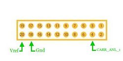
Before running the command in the terminal, you will need to connect the potentiometer to the carrier board as diagrammed. Figure 2 shows where to connect the potentiometer on Header 8 of the SoM-150ES. You will be focusing on CARR_ANL_1 for this example.
Turn the potentiometer counter-clockwise as far as it goes. You'll see the results when you run the command below. Test results will be displayed in the terminal.
root@emac-oe~:$ ./indexed_atod_test /dev/mcp3208-gpio 4
[0] = 83
[1] = 4094
[2] = 61
[3] = 267
The results that are displayed from the terminal show channel 1 analog value at 4094. All the other results are just noise coming from the mcp3208 chip. This noise can be virtually eliminated by grounding the unused A/D inputs.
For the second example, turn the potentiometer clockwise as far as it goes. You'll see how channel 1 results will change when running the command below. Test results will be displayed in the terminal.
root@emac-oe~:$ ./indexed_atod_test /dev/mcp3208-gpio 4
[0] = 62
[1] = 0
[2] = 10
[3] = 95
Here, the results show channel 1 analog value at zero. Your results may vary, depending on the characteristics of your potentiometer and the ADC noise present. You can alter the value by turning the potentiometer to different positions.
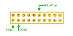
Before doing example 3, you'll want to put the wiper (B) wire on pin 9 of the SoM-150ES carrier board. Figure 3 shows that pin 9 is CARR_ANL_6. Turn the potentiometer counter-clockwise about half way. You'll see how the values on channel 6 will change when running the command below. Test results will be displayed in the terminal.
root@emac-oe~:$ ./indexed_atod_test /dev/mcp3208-gpio 7
[0] = 53
[1] = 0
[2] = 56
[3] = 0
[4] = 29
[5] = 43
[6] = 2044
The results show the channel 6 analog value at 2044, which is about half way (4095/2). You can change any of the channels value with the potentiometer as long as you put the wiper pin on the channel you want to change.
Due to ADC noise, you may see the values fluctuate slightly from one run to the next. This is normal behavior. This fluctuation can be more severe with some potentiometers than it is with others; some potentiometers are more prone to picking up noise. The noise will also be more severe with longer wires, due to transmission line effects. Eliminating noise is typically the greatest challenge in high resolution A/D conversion (especially at 18 bit and above), so you should expect to see some noise when performing an informal test such as this.
Using spi_test
The spi_test program is executed from the console. It takes three parameters.
root@emac-oe~:$ ./spi_test device length mosi
device: Name of thespidevice node.length: Length ofspitransactions in bytes.mosi: Hex value to be transmitted in hexadecimal.
This example command was run on an EMAC SoM-150ES carrier board. Test results will be displayed in the terminal.
root@emac-oe~:$ ./spi_test /dev/mcp3208 3 CDEF
MOSI  MISO
 CD  : 00
 EF  : 01
 FF  : 04
During the SPI clock cycle, the master sends a bit on the MOSI line; the slave then reads it from that line. Next, the slave sends a bit on the MISO line; the master then reads it from that same line.
For this example, we are using an mcp3208 device with a length of 3, and a hex value of CDEF.
root@emac-oe~:$ ./spi_test /dev/mcp3208 4 CCDD
MOSI  MISO
 CD  : 00
 EF  : 01
 FF  : AC
 FF  : 00
When using the same device, but different length and hex value, the results differ.
root@emac-oe~:$ ./spi_test /dev/mcp3208 5 EEFF
MOSI  MISO
 EE  : 00
 FF  : 00
 FF  : F8
 FF  : 00
 FF  : 00
In this third example, the results change again because of the different length and hex value.
Summary
The spi_test C example project demonstrates how to use the SPI device. SPI is simply a way to send data from device to device in a serial fashion (bit by bit). SPI provides good support for communication with peripheral devices that are accessed intermittently. This protocol is used for things like SD memory cards, MP3 decoders, memory devices, and other high speed applications.
SPI can operate at extremely high speeds (million of bytes per second), which may be too fast for some devices. It can also achieve significantly higher data rates than I²C devices or SMBus. SPI is better suited than I²C for applications that are naturally thought of as data streams (as opposed to reading and writing addressed locations in a slave device).

